计算机组成原理上机实验4 有限状态机
2018-04-19
实验目的
综合利用三次实验的结果,完成以下功能:
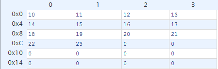
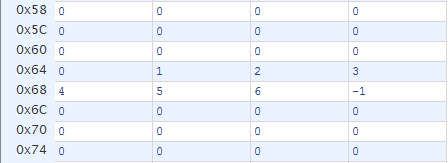
通过例化,向ram中0地址到13地址存入14个数,比如10-23;向ram中100地址到106地址存入7个数,比如0~6,分别代表运算符(与ALU的操作符对应),最后向ram 107地址写入-1
运算控制:
 - 从ram 0地址开始的地方取两个数,分别放在reg0和reg1,然后从ram 100地址开始的地方取一个运算符,放到reg2,计算之后,把结果存入ram地址200

 - 从ram 2地址开始的地方取两个数,分别放在reg0和reg1,从ram 101地址开始的地方取一个运算符,放到reg2,计算之后,把结果存入ram地址201

 - ……

 - 如果取出操作符为-1,则结束。
实验平台
ISE 14.7
实验过程(分析)
模块化设计,一个alu模块,一个regfile模块,一个IP核生成的ram模块,一个control模块,控制reg、ram和alu,顶层一个top模块实例化前几个模块,ram初始化有coe文件读入。
alu模块使用case语句判断7种操作类型。
regfile模块用组合逻辑读,时序逻辑写。
control模块思路(4周期)由于reg在这里没有实质作用(仅是复制了一份存储),故不考虑相关控制
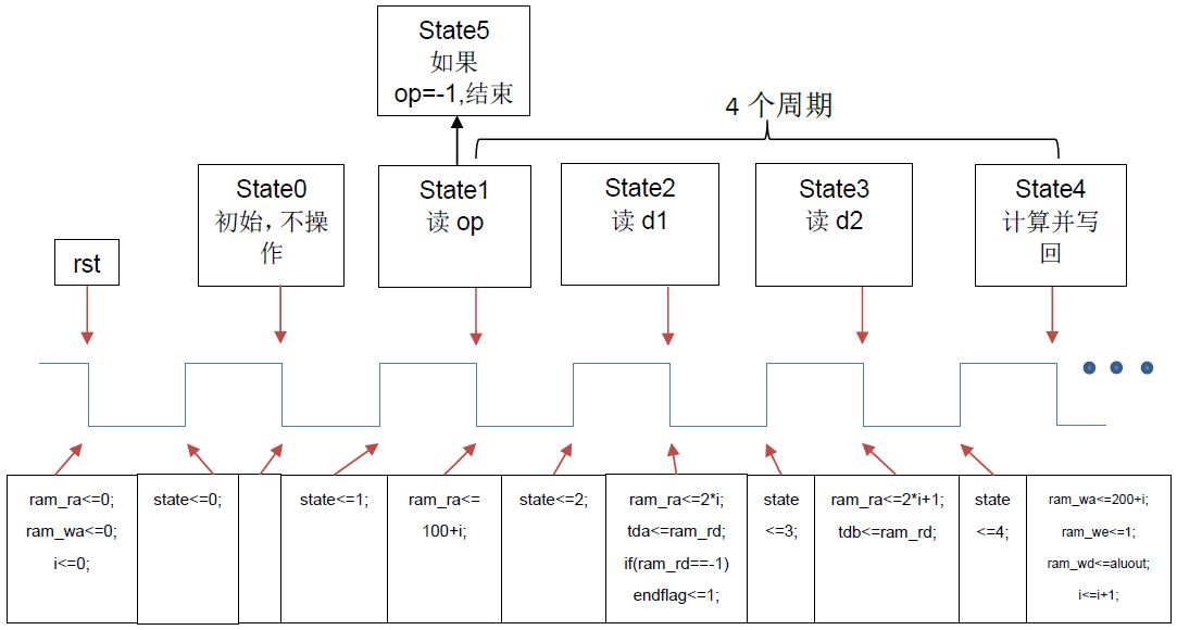
其中ram_ra为ram读地址,ram_rd为ram读数据,ram_we为ram写使能,tda、tdb为临时寄存上一周期的结果。分析结果
Op Data1 Data2 Result 0(nop) 11 10 0 1(add) 13 12 25 2(sub) 15 14 1 3(and) 17(32’b0…10001) 16(32’b0…10000) 16(32’b0…10000) 4(or) 19(32’b0…10011) 18(32’b0…10010) 19(32’b0…10011) 5(xor) 21(32’b0…10101) 20(32’b0…10100) 1(32’b0…00001) 6(nor) 23(32’b0…10111) 22(32’b0…10110) -24(32’b1…101000)
实验结果
仿真结果
IP核ram设置界面中Load In设置ram初始化coe文件的路径,其中文件内容为
  MEMORY_INITIALIZATION_RADIX=10;

  MEMORY_INITIALIZATION_VECTOR=

  10,11,12,13,14,15,16,17,18,19,20,21,22,23,0,0,

  0,0,0,0,0,0,0,0,0,0,0,0,0,0,0,0,

  0,0,0,0,0,0,0,0,0,0,0,0,0,0,0,0,

  0,0,0,0,0,0,0,0,0,0,0,0,0,0,0,0,

  0,0,0,0,0,0,0,0,0,0,0,0,0,0,0,0,

  0,0,0,0,0,0,0,0,0,0,0,0,0,0,0,0,

  0,0,0,0,0,1,2,3,4,5,6,-1,0,0,0,0,

  0,0,0,0,0,0,0,0,0,0,0,0,0,0,0,0,

  0,0,0,0,0,0,0,0,0,0,0,0,0,0,0,0,

  0,0,0,0,0,0,0,0,0,0,0,0,0,0,0,0,

  0,0,0,0,0,0,0,0,0,0,0,0,0,0,0,0,

  0,0,0,0,0,0,0,0,0,0,0,0,0,0,0,0,

  0,0,0,0,0,0,0,0,0,0,0,0,0,0,0,0,

  0,0,0,0,0,0,0,0,0,0,0,0,0,0,0,0,

  0,0,0,0,0,0,0,0,0,0,0,0,0,0,0,0,

  0,0,0,0,0,0,0,0,0,0,0,0,0,0,0,0
仿真得ram和reg数据为
……
……
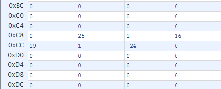
可见计算结果符合分析。
附录:
模块源代码
top.v
module top(
    input clk,
    input rst_n
);

    wire [5:0] ra;
    wire [5:0] wa;
    wire [31:0] rd;
    wire [31:0] wd;
    wire [31:0] aluout;

    reg we=1'b1;
    wire [31:0] tda;
    wire [31:0] tdb;

    wire clkb;
    wire ram_we;
    wire [7:0] ram_ra;
    wire [7:0] ram_wa;
    wire [31:0] ram_rd;
    wire [31:0] ram_wd;

    alu alu1(ram_rd,tdb,tda,aluout);
    regfile regfile1(clk,rst_n,ra,wa,wd,we,rd);
    control control1(clk,rst_n,aluout,ra,rd,wa,wd,tda,tdb,ram_we,ram_ra,ram_rd,ram_wa,ram_wd);
    ram ram1(clk,ram_we,ram_wa,ram_wd,clk,ram_ra,ram_rd);

endmodule
alu.v
parameter A_NOP =5'h00; //nop
parameter A_ADD =5'h01; //sign_add
parameter A_SUB =5'h02; //sign_sub
parameter A_AND =5'h03; //and
parameter A_OR  =5'h04; //or
parameter A_XOR =5'h05; //xor
parameter A_NOR =5'h06; //nor

module alu(
    input [31:0] alu_a,
    input [31:0] alu_b,
    input [4:0] alu_op,
    output reg [31:0] alu_out
    );
    always@(*)
        case (alu_op)
            A_NOP: alu_out = 0;
            A_ADD: alu_out = alu_a + alu_b;
            A_SUB: alu_out = alu_a - alu_b;
            A_AND: alu_out = alu_a & alu_b;
            A_OR : alu_out = alu_a | alu_b;
            A_XOR: alu_out = alu_a ^ alu_b;
            A_NOR: alu_out = ~(alu_a | alu_b);
            default: alu_out = 0;
        endcase
endmodule
regfile.v
module regfile(
    input   clk,
    input rst_n,
    input [5:0] rAddr1,//读地址
    input [5:0] wAddr,//写地址
    input [31:0] wDin,//写数据
    input wEna,//写使能
    output [31:0] rDout1//读数据1
);
    reg [31:0] data [0:63];
    integer i;
    assign rDout1=data[rAddr1];//读

    always@(posedge clk or rst_n)//写和复位
        if(~rst_n)
        begin
            for(i=0; i<64; i=i+1) data[i]<=0;
        end
        else
        begin
            if(wEna)
                data[wAddr]<=wDin;
        end
endmodule
control.v
module control(
    input clk,rst_n,
    input [31:0] aluout,

    output reg [5:0] ra=6'd0,//reg read addr
    input [31:0] rd,//reg read data
    output reg [5:0] wa=6'd0,//reg write addr
    output reg [31:0] wd,//reg write data

    output reg [31:0] tda,//tmp data a
    output reg [31:0] tdb,//tmp data b

    output reg ram_we,//ram write enable
    output reg [7:0] ram_ra,//ram read addr
    input [31:0] ram_rd,//ram read data
    output reg [7:0] ram_wa,//ram write addr
    output reg [31:0] ram_wd//ram write data
    );
    reg [2:0] cstate;//current state
    reg [2:0] nstate;//next state
    reg endflag=0;
    integer i=0;

    always @(posedge clk or negedge rst_n)
        if(~rst_n)
            cstate<=3'd0;
        else
            cstate<=nstate;

    always @(*)
        if(cstate==3'd0) nstate=3'd1;
        else if(cstate==3'd1 & endflag==1'd0) nstate=3'd2;
        else if(cstate==3'd1 & endflag==1'd1) nstate=3'd5;
        else if(cstate==3'd2) nstate=3'd3;
        else if(cstate==3'd3) nstate=3'd4;
        else if(cstate==3'd4) nstate=3'd1;
        else if(cstate==3'd5) nstate=3'd5;
    always @(negedge clk or negedge rst_n)
    begin
        if(~rst_n)
            begin
                ram_ra<=0;
                ram_wa<=0;
                i<=0;
            end
        else if(cstate==3'd1)
            begin
                ram_ra<=100+i;
            end
        else if(cstate==3'd2)
            begin
                ram_ra<=2*i;
                tda<=ram_rd;
                if(ram_rd==-1) endflag<=1;
            end
        else if(cstate==3'd3)
            begin
                ram_ra<=2*i+1;
                tdb<=ram_rd;
            end
        else if(cstate==3'd4)
            begin
                ram_wa<=200+i;
                ram_we<=1;
                ram_wd<=aluout;
                i<=i+1;
            end
    end

endmodule
test.v
module test(
    );
    reg clk,rst_n;
    top test(
        .clk(clk),
        .rst_n(rst_n),
    );
    always #10 clk=~clk;
    initial begin
        clk=0;
        rst_n=0;
        #20;
        rst_n=1;
    end
endmodule